Continue to site >>>


Altera DE2-115 Development Board
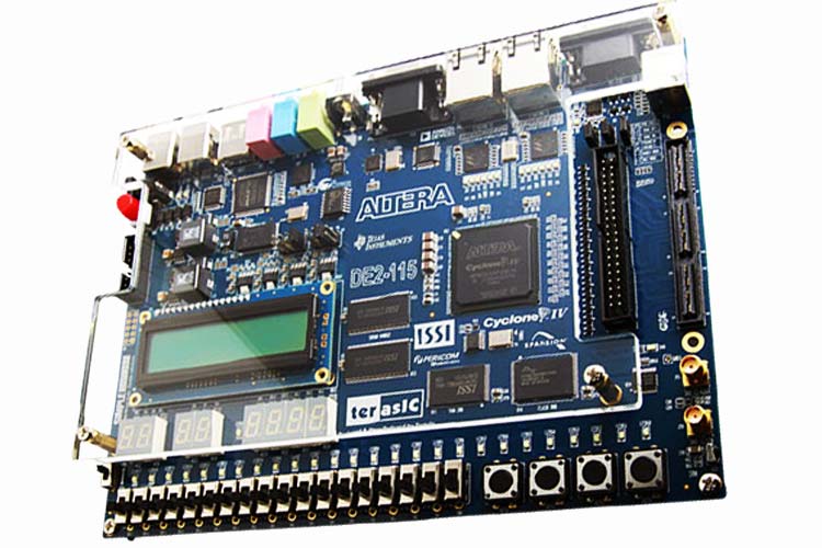
[Click the image to enlarge it]
The DE2 series has consistently been at the forefront of educational development boards by distinguishing itself with an abundance of interfaces to accommodate various application needs. Extending its leadership and success, Terasic announces the latest DE2-115 that features the Cyclone IV E device . Responding to increased versatile low-cost spectrum needs to be driven by the demand for mobile video, voice, data access, and the hunger for high-quality images, the new DE2-115 offers an optimal balance of low cost, low power, and a rich supply of logic, memory, and DSP capabilities .
Altera DE2-115 Development Board Pinout
The DE2-115 Board provides one 40-pin expansion header. The header connects directly to 36 pins of the Cyclone IV E FPGA and also provides DC +5V (VCC5), DC +3.3V (VCC3P3), and two GND pins.
| Signal Name | FPGA Pin No | Description | I/O Standard |
| GPIO[0] | PIN_AB22 | GPIO Connection DATA[0] | Depending on JP6 |
| GPIO[1] | PIN_AC15 | GPIO Connection DATA[1] | Depending on JP6 |
| GPIO[2] | PIN_AB21 | GPIO Connection DATA[2] | Depending on JP6 |
| GPIO[3] | PIN_Y17 | GPIO Connection DATA[3] | Depending on JP6 |
| GPIO[4] | PIN_AC21 | GPIO Connection DATA[4 | Depending on JP6 |
| GPIO[5] | PIN_Y16 | GPIO Connection DATA[5] | Depending on JP6 |
| GPIO[6] | PIN_AD21 | GPIO Connection DATA[6] | Depending on JP6 |
| GPIO[7] | PIN_AE16 | GPIO Connection DATA[7] | Depending on JP6 |
| GPIO[8] | PIN_AD15 | GPIO Connection DATA[8] | Depending on JP6 |
| GPIO[9] | PIN_AE15 | GPIO Connection DATA[9] | Depending on JP6 |
| GPIO[10] | PIN_AC19 | GPIO Connection DATA[10] | Depending on JP6 |
| GPIO[11] | PIN_AF16 | GPIO Connection DATA[11] | Depending on JP6 |
| GPIO[12] | PIN_AD19 | GPIO Connection DATA[12] | Depending on JP6 |
| GPIO[13] | PIN_AF15 | GPIO Connection DATA[13] | Depending on JP6 |
| GPIO[14] | PIN_AF24 | GPIO Connection DATA[14] | Depending on JP6 |
| GPIO[15] | PIN_AE21 | GPIO Connection DATA[15] | Depending on JP6 |
| GPIO[16] | PIN_AF25 | GPIO Connection DATA[16] | Depending on JP6 |
| GPIO[17] | PIN_AC22 | GPIO Connection DATA[17] | Depending on JP6 |
| GPIO[18] | PIN_AE22 | GPIO Connection DATA[18] | Depending on JP6 |
| GPIO[19] | PIN_AF21 | GPIO Connection DATA[19] | Depending on JP6 |
| GPIO[20] | PIN_AF22 | GPIO Connection DATA[20] | Depending on JP6 |
| GPIO[21] | PIN_AD22 | GPIO Connection DATA[21] | Depending on JP6 |
| GPIO[22] | PIN_AG25 | GPIO Connection DATA[22] | Depending on JP6 |
| GPIO[23] | PIN_AD25 | GPIO Connection DATA[23] | Depending on JP6 |
| GPIO[24] | PIN_AH25 | GPIO Connection DATA[24] | Depending on JP6 |
| GPIO[25] | PIN_AE25 | GPIO Connection DATA[25] | Depending on JP6 |
| GPIO[26] | PIN_AG22 | GPIO Connection DATA[26] | Depending on JP6 |
| GPIO[27] | PIN_AE24 | GPIO Connection DATA[27] | Depending on JP6 |
| GPIO[28] | PIN_AH22 | GPIO Connection DATA[28] | Depending on JP6 |
| GPIO[29] | PIN_AF26 | GPIO Connection DATA[29] | Depending on JP6 |
| GPIO[30] | PIN_AE20 | GPIO Connection DATA[30] | Depending on JP6 |
| GPIO[31] | PIN_AG23 | GPIO Connection DATA[31] | Depending on JP6 |
| GPIO[32] | PIN_AF20 | GPIO Connection DATA[32] | Depending on JP6 |
| GPIO[33] | PIN_AH26 | GPIO Connection DATA[33] | Depending on JP6 |
| GPIO[34] | PIN_AH23 | GPIO Connection DATA[34 | Depending on JP6 |
| GPIO[35] | PIN_AG26 | GPIO Connection DATA[35] | Depending on JP6 |
Features and Specifications
- Altera Cyclone® IV 4CE115 FPGA device
- Altera Serial Configuration device – EPCS64
- USB Blaster (onboard) for programming; both JTAG and Active Serial (AS) programming modes are supported
- 2MB SRAM
- Two 64MB SDRAM
- 8MB Flash memory
- SD Card socket
- 4 Push-buttons
- 18 Slide switches
- 18 Red user LEDs
- 9 Green user LEDs
- 50MHz oscillator for clock sources
- 24-bit CD-quality audio CODEC with line-in, line-out, and microphone-in jacks
- VGA DAC (8-bit high-speed triple DACs) with VGA-out connector
- TV Decoder (NTSC/PAL/SECAM) and TV-in connector
- 2 Gigabit Ethernet PHY with RJ45 connectors
- USB Host/Slave Controller with USB type A and type B connectors
- RS-232 transceiver and 9-pin connector
- PS/2 mouse/keyboard connector
- IR Receiver
- 2 SMA connectors for external clock input/output
- One 40-pin Expansion Header with diode protection
- One High-Speed Mezzanine Card (HSMC) connector
- 16x2 LCD module
In addition to these hardware features, the DE2-115 board has software support for standard I/O interfaces and a control panel facility for accessing various components. Also, the software is provided for supporting a number of demonstrations that illustrate the advanced capabilities of the DE2-115 board.
Note: To know more about specific features in detail, check out the DE2-115 board datasheet given at the bottom of this page.
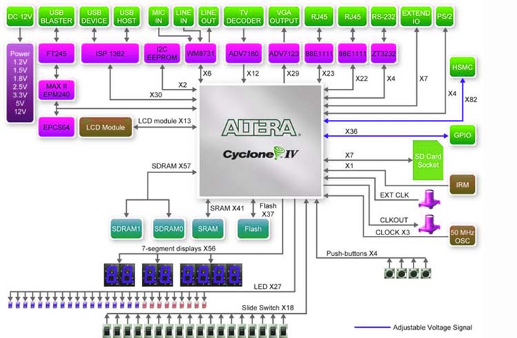
DE2-115 Board Block Diagram
The basic block diagram of the DE2-115 board is shown below. You can check out the datasheet for more info on the device.
Power up the DE2-115 Board
The DE2-115 board comes with a preloaded configuration bitstream to demonstrate some features of the board. This bitstream also allows users to see quickly if the board is working properly.
To power up the board, perform the following steps:
1. Connect the provided USB cable from the host computer to the USB Blaster connector on the DE2-115 board. For communication between the host and the DE2-115 board, it is necessary to install the Altera USB Blaster driver software. If this driver is not already installed on the host computer, it can be installed as explained in the tutorial “ Getting Started with Altera's DE2-115 Board ” (DE2-115 board datasheet) which is linked on the bottom of the page. This tutorial is available in the directory DE2_115_tutorials on the DE2-115 System CD.
2. Turn off the power by pressing the red ON/OFF switch before connecting the 12V adapter to the DE2-115 board.
3. Connect a VGA monitor to the VGA port on the DE2-115 board.
4. Connect your headset to the line-out audio port on the DE2-115 board.
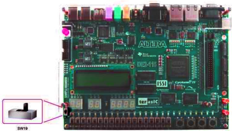
5. Turn the RUN/PROG switch (SW19) on the left edge of the DE2-115 board to the RUN position; the PROG position is used only for the AS Mode programming.
6. Recycle the power by turning the red power switch (on the DE2-115 board) OFF and ON again.
At this point you should observe the following:
- All user LEDs are flashing
- All 7-segment displays are cycling through the numbers 0 to F
- The LCD display shows “Welcome to the Altera DE2-115”
- The VGA monitor displays the image shown in Figure 2-4
- Set the slide switch SW17 to the DOWN position; you should hear a 1-kHz sound. Be careful of loud volume for avoiding any discomfort
- Set the slide switch SW17 to the UP position and connect the output of an audio player to the line-in connector on the DE2-115 board; on your speaker or headset you should hear the music played from the audio player (MP3, PC, iPod, or the like)
- You can also connect a microphone to the microphone-in connector on the DE2-115 board; your voice will be mixed with the music playing on the audio player.
The DE2-115 board comes with a Control Panel facility that allows users to access various components on the board from a host computer. The host computer communicates with the board through a USB connection. The facility can be used to verify the functionality of components on the board or be used as a debug tool while developing RTL code. This chapter first presents some basic functions of the Control Panel, then describes its structure in block diagram form, and finally describes its capabilities
JTAG Chain on DE2-115 Board
To use the JTAG interface for configuring an FPGA device, the JTAG chain on DE2-115 must form a close loop that allows the Quartus II programmer to detect the FPGA device. Shorting pin1 and pin2 on JP3 can disable the JTAG signals on the HSMC connector that will form a close JTAG loop chain on the DE2-115 board. To do that you need to flip the switch SW19 on the board to enable JTAG.
Applications
- high-speed search
- aerospace and defense
- medical electronics
- digital television
- consumer electronics
- industrial motor control
- scientific instruments
- cybersecurity systems, and wireless communications
Lab 2: Introduction to Altera DE2 Board
Objectives:.
The objective of this experiment is to gain an understanding of the Altera DE2 Board and create a simple project using input switches and the output LEDs.
Preparation
- Review the provided user manual and tutorials for the Altera DE2 Board
Equipment Needed
- ALTERA DE2 Board
- User manual for Altera DE2 Board
A field programmable gate array (FPGA) is a semiconductor device containing programmable logic components and programmable interconnects. The programmable logic components can be programmed to duplicate the functionality of basic logic gates such as AND, OR, XOR, NOT or more complex combinational functions such as decoders or simple math functions. In most FPGAs, these programmable logic components also include memory elements, which may be simple flip flops or more complete blocks of memories
For this course we will be using a programming language called VHDL to program the FPGA found on the Cyclone 2 chip on your Altera DE2 Board. VHDL is a very robust language that can be implemented in a very high level format, using programming concepts such as for loops, if-then statements, and case assignments. VHDL also includes libraries that define adders, subtracters, counters, flip-flops, and more that can be instantiated to create a structural approach to your code.
The purpose of this exercise is to learn how to connect simple input and output devices to an FPGA chip and implement a circuit that uses these devices. We will use the switches SW 17−0 on the DE2 board as inputs to the circuit. We will use light emitting diodes (LEDs) as outputs to your device.
The DE2 board provides 18 toggle switches, called SW 17−0 , which can be used as inputs to a circuit. There are also 18 red LEDs, called LEDR 17−0 , which can be used to display output values. The DE2 board has hardwired connections between its FPGA chip and the switches and lights. To use SW 17−0 and LEDR 17−0 it is necessary to include in your Quartus II project the correct pin assignments, which are given in the DE2 User Manual.
Figure 2.1 shows a sum-of-products circuit that implements a 2-to-1 multiplexer with a select input s. If s = 0 the multiplexer’s output m is equal to the input x, and if s = 1 the output is equal to y. Part (b) of the figure gives a truth table for this multiplexer, and part (c) shows its circuit symbol.
| | Figure 2.1: A 2-to-1 multiplexer The multiplexer can be described by the following VHDL statement: m <= (NOT (s) AND x) OR (s AND y); You are to use the provided VHDL entity in appendix 2.1 that describes the circuit given in Figure 3a. This circuit has two eight-bit inputs, X and Y, and produces the eight-bit output M. If s = 0 then M = X, while if s = 1 then M = Y. We refer to this circuit as an eight-bit wide 2-to-1 multiplexer. It has the circuit symbol shown in Figure 3b, in which X, Y, and M are depicted as eight-bit wires. In Figure 2.1 we showed a 2-to-1 multiplexer that selects between the two inputs x and y. For this part consider a circuit in which the output m has to be selected from five inputs u, v, w, x, and y. Part (a) of Figure 2.3 shows how we can build the required 5-to-1 multiplexer by using four 2-to-1 multiplexers. The circuit uses a 3-bit select input s2s1s0 and implements the truth table shown in Figure 4b. A circuit symbol for this multiplexer is given in part (c) of the figure. | | | s | s | s | m | | 0 | 0 | 0 | u | | 0 | 0 | 1 | v | | 0 | 1 | 0 | w | | 0 | 1 | 1 | x | | 1 | 0 | 0 | y | | 1 | 0 | 1 | y | | 1 | 1 | 0 | y | | 1 | 1 | 1 | y | Recall from Figure 2.2 that an eight-bit wide 2-to-1 multiplexer can be built by using eight instances of a 2-to-1 multiplexer. Figure 2.4 applies this concept to define a three-bit wide 5-to-1 multiplexer. It contains three instances of the circuit in Figure 4a. The VHDL code for this circuit is given in appendix 2.1 Prelab Assignments- Review the manual and tutorials for the Altera DE2 Board.
- Understand how to create and compile projects.
- Review how pin assignments are done.
- Review how to program the Altera DE2 Board.
Lab Assignments- Create a new Quartus II project for your circuit.
- Include the given VHDL code for the eight-bit wide 2-to-1 multiplexer in your project. Use switch SW17 on the DE2 board as the s input, switches SW7−0 as the X input and SW15−8 as the Y input. Connect the SW switches to the red lights LEDR and connect the output M to the green lights LEDG7−0.
- Include in your project the required pin assignments for the DE2 board.
- Compile the project.
- Download the compiled circuit into the FPGA chip. Test the functionality of the eight-bit wide 2-to-1 multiplexer by toggling the switches and observing the LEDs.
- Include the given VHDL code for the three-bit wide 5-to-1 multiplexer. Connect its select inputs to switches SW17−15, and use the remaining 15 switches SW14−0 to provide the five 3-bit inputs U to Y. Connect the SW switches to the red lights LEDR and connect the output M to the green lights LEDG2−0.
- Include in your project the required pin assignments for the DE2 board. Compile the project.
- Download the compiled circuit into the FPGA chip. Test the functionality of the three-bit wide 5-to-1 multiplexer by toggling the switches and observing the LEDs. Ensure that each of the inputs U to Y can be properly selected as the output M.
 - Altera Manuals
- Computer Hardware
- User manual
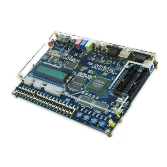
Altera DE2-70 User ManualTable of ContentsChapter 1 de2-70 package. - Package Contents
- The DE2-70 Board Assembly
- Getting Help
Chapter 2 Altera DE2-70 Board- Layout and Components
- Block Diagram of the DE2-70 Board
- Power-Up the DE2-70 Board
Chapter 3 DE2-70 Control Panel- Control Panel Setup
- Controlling the Leds, 7-Segment Displays and LCD Display
- Switches and Buttons
- Sdram/Ssram/Flash Controller and Programmer
- USB Monitoring
- Audio Playing and Recording
- Overall Structure of the DE2-70 Control Panel
Chapter 4 DE2-70 Video Utility- Video Utility Setup
- VGA Display
- Video Capture
- Overall Structure of the DE2-70 Video Utility
Chapter 5 Using the DE2-70 Board- Configuring the Cyclone II FPGA
- Using the Leds and Switches
- Using the 7-Segment Displays
- Clock Circuitry
- Using the LCD Module
- Using the Expansion Header
- Using the 24-Bit Audio CODEC
- RS-232 Serial Port
- PS/2 Serial Port
- Fast Ethernet Network Controller
- Implementing a TV Encoder
- Using USB Host and Device
- Using Sdram/Sram/Flash
Chapter 6 Examples of Advanced Demonstrations- DE2-70 Factory Configuration
- TV Box Demonstration
- TV Box Picture in Picture (PIP) Demonstration
- USB Paintbrush
- A Karaoke Machine
- Ethernet Packet Sending/Receiving
- SD Card Music Player
- Music Synthesizer Demonstration
- Audio Recording and Playing
Chapter 7 Appendix- Revision History
- Copyright Statement
Advertisement Quick Links- 1 Package Contents
- 2 Layout and Components
- 3 Using the Leds and Switches
- 4 Using the 7-Segment Displays
- 5 Using the Lcd Module
- Download this manual
Related Manuals for Altera DE2-70 Summary of Contents for Altera DE2-70- Page 1 Altera DE2-70 Board Version 1.01 Copyright © 2007 Terasic Technologies...
Page 2: Table Of Contents- Page 3 Using USB Host and Device...55 5.15 Using IrDA...56 5.16 Using SDRAM/SRAM/Flash...57 Chapter 6 Examples of Advanced Demonstrations ...66 DE2-70 Factory Configuration ...66 TV Box Demonstration...67 TV Box Picture in Picture (PIP) Demonstration...69 USB Paintbrush...72 USB Device...74 A Karaoke Machine ...76 Ethernet Packet Sending/Receiving ...78...
Page 4: Chapter 1 De2-70 PackagePage 5: the de2-70 board assembly, page 6: getting help, page 7: chapter 2 altera de2-70 board, page 8: block diagram of the de2-70 board. - Page 9 Figure 2.2. Block diagram of the DE2-70 board. Following is more detailed information about the blocks in Figure 2.2: Cyclone II 2C70 FPGA • 68,416 LEs • 250 M4K RAM blocks • 1,152,000 total RAM bits • 150 embedded multipliers •...
- Page 10 • Normally high; generates one active-low pulse when the switch is pressed Toggle switches • 18 toggle switches for user inputs • A switch causes logic 0 when in the DOWN (closest to the edge of the DE2-70 board) position and logic 1 when in the UP position Clock inputs •...
- Page 11 Audio CODEC • Wolfson WM8731 24-bit sigma-delta audio CODEC • Line-level input, line-level output, and microphone input jacks • Sampling frequency: 8 to 96 KHz • Applications for MP3 players and recorders, PDAs, smart phones, voice recorders, etc. VGA output •...
Page 12: Power-Up The De2-70 Board- Page 13 • Set the toggle switch SW17 to the UP position and connect the output of an audio player to the Line-in connector on the DE2-70 board; on your headset you should hear the music played from the audio player (MP3, PC, iPod, or the like) •...
Page 14: Chapter 3 De2-70 Control Panel- Page 15 7. The Control Panel is now ready for use; experiment by setting the value of some LEDs display and observing the result on the DE2-70 board. The concept of the DE2-70 Control Panel is illustrated in Figure 3.2. The “Control Codes” that performs the control functions is implemented in the FPGA board. It communicates with the Control Panel window, which is active on the host computer, via the USB Blaster link.
Page 16: Controlling The Leds, 7-Segment Displays And Lcd Display- Page 17 DE2-70 User Manual Figure 3.3. Controlling LEDs. Choosing the 7-SEG tab leads to the window in Figure 3.4. In the tab sheet, directly use the Up-Down control and Dot Check box to specified desired patterns, the 7-SEG patterns on the board will be updated immediately.
Page 18: Switches And ButtonsPage 19: sdram/ssram/flash controller and programmer. - Page 20 ASCII text files that specify memory values using ASCII characters to represent hexadecimal values. For example, a file containing the line defines four 8-bit values: 01, 23, 45, 67, 89, AB, CD, EF. These values will be loaded consecutively 0123456789ABCDEF DE2-70 User Manual...
Page 21: Usb MonitoringPage 22: ps2 device, page 23: sd card, page 24: audio playing and recording. - Page 25 4. To stop recording, click “Stop Record”. Finally, audio signal saved in SDRAM-U1 will be uploaded to the host computer and displayed on the waveform window. Click “Save Wave” to save the waveform into a WAV file. DE2-70 User Manual...
Page 26: Overall Structure Of The De2-70 Control Panel- Page 27 FPGA/ SOPC NIOS II TIMER JTAG JTAG Blaster Hardware Figure 3.13. The block diagram of the DE2-70 control panel. SEG7 Controller SDRAM Controller SDRAM Controller LCD Controller USB Controller PS2 Controller PIO Controller Avalon- MM Flash Controller Tris tate Bridge...
Page 28: Chapter 4 De2-70 Video UtilityPage 29: vga display, page 30: video capture, page 31: overall structure of the de2-70 video utility. - Page 32 Host computer converts the raw image data to RGB color space and displays it. SDRAM Controller SDRAM Controller Controller Multi - Port SSRAM Controller Avalon MM Slave VIDEO-In Controller DE2-70 User Manual NIOS II Program SDRAM-U1 SDRAM-U2 SSRAM VIDEO IN...
Page 33: Chapter 5 Using The De2-70 Board- Page 34 Cyclone II FPGA, perform the following steps: • Ensure that power is applied to the DE2-70 board • Connect the supplied USB cable to the USB Blaster port on the DE2-70 board (see Figure 2.1) • Configure the JTAG programming circuit by setting the RUN/PROG switch (on the left side of the board) to the RUN position.
Page 35: Using The Leds And Switches- Page 36 DE2-70 User Manual There are also 18 toggle switches (sliders) on the DE2-70 board. These switches are not debounced, and are intended for use as level-sensitive data inputs to a circuit. Each switch is connected directly to a pin on the Cyclone II FPGA. When a switch is in the DOWN position (closest to the edge of the board) it provides a low logic level (0 volts) to the FPGA, and when the switch is in the UP position it provides a high logic level (3.3 volts).
- Page 37 SW[14] PIN_L5 SW[15] PIN_L4 Description Toggle Switch[0] Toggle Switch[1] Toggle Switch[2] Toggle Switch[3] Toggle Switch[4] Toggle Switch[5] Toggle Switch[6] Toggle Switch[7] Toggle Switch[8] Toggle Switch[9] Toggle Switch[10] Toggle Switch[11] Toggle Switch[12] Toggle Switch[13] Toggle Switch[14] Toggle Switch[15] DE2-70 User Manual...
- Page 38 LED Red[6] LED Red[7] LED Red[8] LED Red[9] LED Red[10] LED Red[11] LED Red[12] LED Red[13] LED Red[14] LED Red[15] LED Red[16] LED Red[17] LED Green[0] LED Green[1] LED Green[2] LED Green[3] LED Green[4] LED Green[5] LED Green[6] DE2-70 User Manual...
Page 39: Using The 7-Segment Displays- Page 40 Seven Segment Decimal Point 3 Seven Segment Digit 4[0] Seven Segment Digit 4[1] Seven Segment Digit 4[2] Seven Segment Digit 4[3] Seven Segment Digit 4[4] Seven Segment Digit 4[5] Seven Segment Digit 4[6] Seven Segment Decimal Point 4 DE2-70 User Manual...
Page 41: Clock Circuitry- Page 42 Cyclone II FPGA SDRAM SSRAM Description 28 MHz clock input 50 MHz clock input 50 MHz clock input 50 MHz clock input 50 MHz clock input External (SMA) clock input DE2-70 User Manual SD Card AUDIO CODEC PS/2 Ethernet FLASH...
 Page 43: Using The Lcd ModulePage 44: using the expansion header. - Page 45 Figure 5.11. Schematic diagram of the expansion headers. Signal Name FPGA Pin No. IO_A [0] PIN_C30 IO_A [1] PIN_C29 IO_A [2] PIN_E28 1.8V 2.5V 3.3V Description GPIO Connection 0 IO[0] GPIO Connection 0 IO[1] GPIO Connection 0 IO[2] DE2-70 User Manual...
- Page 46 GPIO Connection 0 IO[31] GPIO Connection 0 PLL In GPIO Connection 0 PLL In GPIO Connection 0 PLL Out GPIO Connection 0 PLL Out GPIO Connection 1 IO[0] GPIO Connection 1 IO[1] GPIO Connection 1 IO[2] GPIO Connection 1 IO[3] DE2-70 User Manual...
- Page 47 GPIO Connection 1 IO[27] GPIO Connection 1 IO[28] GPIO Connection 1 IO[29] GPIO Connection 1 IO[30] GPIO Connection 1 IO[31] GPIO Connection 1 PLL In GPIO Connection 1 PLL In GPIO Connection 1 PLL Out GPIO Connection 1 PLL Out DE2-70 User Manual...
Page 48: Using Vga- Page 49 Datasheet/VGA DAC folder on the DE2-70 System CD-ROM. The pin assignments between the Cyclone II FPGA and the ADV7123 are listed in Table 5.11. An example of code that drives a VGA display is described in Sections 6.2, 6.3 and 6.4.
- Page 50 VGA Green[6] VGA Green[7] VGA Green[8] VGA Green[9] VGA Blue[0] VGA Blue[1] VGA Blue[2] VGA Blue[3] VGA Blue[4] VGA Blue[5] VGA Blue[6] VGA Blue[7] VGA Blue[8] VGA Blue[9] VGA Clock VGA BLANK VGA H_SYNC VGA V_SYNC VGA SYNC DE2-70 User Manual...
Page 51: Using The 24-Bit Audio CodecPage 52: rs-232 serial port, page 53: fast ethernet network controller. - Page 54 Description DM9000A DATA[0] DM9000A DATA[1] DM9000A DATA[2] DM9000A DATA[3] DM9000A DATA[4] DM9000A DATA[5] DM9000A DATA[6] DM9000A DATA[7] DM9000A DATA[8] DM9000A DATA[9] DM9000A DATA[10] DM9000A DATA[11] DM9000A DATA[12] DM9000A DATA[13] DM9000A DATA[14] DM9000A DATA[15] DM9000A Clock 25 MHz DE2-70 User Manual...
Page 55: Tv Decoder- Page 56 TV Decoder 1 Data[0] TV Decoder 1 Data[1] TV Decoder 1 Data[2] TV Decoder 1 Data[3] TV Decoder 1 Data[4] TV Decoder 1 Data[5] TV Decoder 1 Data[6] TV Decoder 1 Data[7] TV Decoder 1 H_SYNC TV Decoder 1 V_SYNC DE2-70 User Manual...
Page 57: Implementing A Tv EncoderPage 58: using usb host and device, page 59: using irda, page 60: using sdram/sram/flash. - Page 61 DE2-70 User Manual Figure 5.22. SDRAM schematic.
- Page 62 RESET# FLASH_WP_n WP#ACC FLASH_RY RY/BY# FLASH_CE_n FLASH_OE_n FLASH_BYTE_n BYTE# F_VCC33 4.7K 4.7K FLASH_RY 4.7K 4.7K FLASH_CE_n Figure 5.24. Flash schematic. DE2-70 User Manual SRAM_data0 DQA0 SRAM_data1 DQA1 SRAM_data2 DQA2 SRAM_data3 DQA3 SRAM_data4 DQA4 SRAM_data5 DQA5 SRAM_data6 DQA6 SRAM_data7 DQA7 SRAM_datapar0...
- Page 63 SDRAM 1 Data[13] SDRAM 1 Data[14] SDRAM 1 Data[15] SDRAM 1 Bank Address[0] SDRAM 1 Bank Address[1] SDRAM 1 Low-byte Data Mask SDRAM 1 High-byte Data Mask SDRAM 1 Row Address Strobe SDRAM 1 Column Address Strobe DE2-70 User Manual...
- Page 64 SDRAM 2 Data[9] SDRAM 2 Data[10] SDRAM 2 Data[11] SDRAM 2 Data[12] SDRAM 2 Data[13] SDRAM 2 Data[14] SDRAM 2 Data[15] SDRAM 2 Bank Address[0] SDRAM 2 Bank Address[1] SDRAM 2 Low-byte Data Mask SDRAM 2 High-byte Data Mask DE2-70 User Manual...
- Page 65 SRAM Address[8] SRAM Address[9] SRAM Address[10] SRAM Address[11] SRAM Address[12] SRAM Address[13] SRAM Address[14] SRAM Address[15] SRAM Address[16] SRAM Address[17] SRAM Address[18] SRAM Data[0] SRAM Data[1] SRAM Data[2] SRAM Data[3] SRAM Data[4] SRAM Data[5] SRAM Data[6] SRAM Data[7] DE2-70 User Manual...
- Page 66 SRAM Burst Address Advance SRAM Byte Write Enable[0] SRAM Byte Write Enable[1] SRAM Byte Write Enable[2] SRAM Byte Write Enable[3] SRAM Chip Enable 1 SRAM Chip Enable 2 SRAM Chip Enable 3 SRAM Clock SRAM Parity Data[0] SRAM Parity Data[1] DE2-70 User Manual...
- Page 67 FLASH Address[8] FLASH Address[9] FLASH Address[10] FLASH Address[11] FLASH Address[12] FLASH Address[13] FLASH Address[14] FLASH Address[15] FLASH Address[16] FLASH Address[17] FLASH Address[18] FLASH Address[19] FLASH Address[20] FLASH Address[21] FLASH Data[0] FLASH Data[1] FLASH Data[2] FLASH Data[3] FLASH Data[4] DE2-70 User Manual...
- Page 68 FLASH Data[9] FLASH Data[10] FLASH Data[11] FLASH Data[12] FLASH Data[13] FLASH Data[14] FLASH Data[15] FLASH Byte/Word Mode Configuration FLASH Chip Enable FLASH Output Enable FLASH Reset LASH Ready/Busy output FLASH Write Enable FLASH Write Protect /Programming Acceleration DE2-70 User Manual...
Page 69: Chapter 6 Examples Of Advanced DemonstrationsPage 70: tv box demonstration. - Page 71 4:3 aspect ratio o Non-progressive video • Connect the VGA output of the DE2-70 board to a VGA monitor (both LCD and CRT type of monitors should work) • Connect the audio output of the DVD player to the line-in port of the DE2-70 board and connect a speaker to the line-out port.
Page 72: Tv Box Picture In Picture (Pip) Demonstration- Page 73 • Connect the one audio output of the DVD player to the line-in port of the DE2-70 board and connect a speaker to the line-out port. If the audio output jacks from the DVD player are of...
- Page 74 RCA type, then an adaptor will be needed to convert to the mini-stereo plug supported on the DE2-70 board; this is the same type of plug supported on most computers • Load the bit stream into FPGA. • The detailed configuration for switching video source of main and sub window are listed in Table 6.1.
Page 75: Usb Paintbrush- Page 76 Nios II Workspace: DE2_70_NIOS_HOST_MOUSE_VGA\Software • Connect a USB Mouse to the USB Host Connector (type A) of the DE2-70 board • Connect the VGA output of the DE2-70 board to a VGA monitor (both LCD and CRT type of monitors should work) •...
Page 77: Usb Device- Page 78 • Nios II Workspace: DE2_70_NIOS_DEVICE_LED\HW\Software • Borland BC++ Software Driver: DE2_70_NIOS_DEVICE_LED\SW • Connect the USB Device connector of the DE2-70 board to the host computer using a USB cable (type A → B). • Load the bit stream into FPGA •...
Page 79: A Karaoke Machine- Page 80 • Project directory: DE2-70_i2sound • Bit stream used: DE2-70_i2sound.sof or DE2-70_i2sound.pof • Connect a microphone to the microphone-in port (pink color) on the DE2-70 board • Connect the audio output of a music-player, such as an MP3 player or computer, to the line-in port (blue color) on the DE2-70 board •...
Page 81: Ethernet Packet Sending/Receiving- Page 82 MAC address of the DE2-70 board. If the packet received does have the same MAC address or is a broadcast packet, the DM9000A will accept the packet and send an interrupt to the Nios II processor. The processor will then display the packet contents in the Nios II IDE console window.
Page 83: Sd Card Music Player- Page 84 DE2-70 User Manual Figure 6.13 shows the hardware block diagram of this demonstration. The system requires a 50 MHZ clock provided from the board. The PLL generates a 100-MHZ clock for NIOS II processor and the other controllers except for the audio controller. The audio chip is controlled by the Audio Controller which is a user-defined SOPC component.
- Page 85 • Load the bitstream into the FPGA on the DE2-70 board. • Run the Nios II IDE under the workspace DE2_70_SD_Card_Audio_Playe\Software • Connect a headset or speaker to the DE2-70 board and you should be able to hear the music played from the SD Card...
Page 86: Music Synthesizer Demonstration- Page 87 SW9. To repeat the demo sound, users can press KEY1. The TONE_GENERATOR has two tones: (1) String. (2) Brass, which can be controlled by SW0. The audio codec used on the DE2-70 board has two channels, which can be turned ON/OFF using SW1 and SW2.
- Page 88 • Bit stream used: DE2_70_Synthesizer.sof or DE2-70_Synthesizer.pof • Connect a PS/2 Keyboard to the DE2-70 board. • Connect the VGA output of the DE2-70 board to a VGA monitor (both LCD and CRT type of monitors should work) • Connect the Lineout of the DE2-70 board to a speaker.
- Page 89 Figure 6.16. The Setup of the Music Synthesizer Demonstration. C D E F G A B C D E F G A B C D E F G A B VGA(LCD/CRT)Monitor VGA Out Keyboard Input Keyboard Algorithms for Audio Processing DE2-70 User Manual...
Page 90: Audio Recording And Playing- Page 91 • Software Project directory: DE2_70_AUDIO\software\project_audio • Software Execution File: DE2_70_AUDIO\software\project_auido\audio\debug\audio.elf • Connect an Audio Source to the LINE-IN port of the DE2-70 board. • Connect a Microphone to MIC-IN port on the DE2-70 board. • Connect a speaker or headset to LINE-OUT port on the DE2-70 board.
- Page 92 • Load the Software Execution File into FPGA. ( • Configure audio with the toggle switches. • Press KEY3 on the DE2-70 board to start/stop audio recoding ( • Press KEY2 on the DE2-70 board to start/stop audio playing ( Note: (1).
Page 93: Chapter 7 AppendixRename the bookmark, delete bookmark, delete from my manuals, upload manual. Mechanics of Altera DE2 Projects | |
| Setup projectImport assignments. | The DE2 board has a default set of pin assignments (and associated pin names) in . Your life will be much easier if you import this file and use the variable names assigned by the developer. |
| Compile ProjectProgram the de2 board. | Make sure the USB cable is in place, and USB Blaster is the selected device. Check the box if not already checked. If the USB Blaster is not the selected hardware device, you can press the button |
| | Hardware Setup | This dialog allows you to select a programming hardware setup to use when programming devices. The button labeled is used to add a new hardware driver, to add a new selection. Just select a hardware configuration from the list to highlight it, then press the button. |
| | Maintained by John Loomis , last updated 18 January 2008  Altera DE2-115 Development and Education Board- 1. Overview
- 2. Specifications
- 3. Layout
- 4. Resources
- 5. Kit Contents
- 6. Applications
- 7. Order Now
Reference Book: Modern Digital Designs with EDA, VHDL and FPGA | Title | Version | Size | Date | Download |
|---|
| DE2-115 User Manual | 2.3 | 14,048(KB) | 2017-08-14 | | | DE2-115_FAQ_v1.1 | | 198(KB) | 2012-06-07 | | | Title | Version | Size | Date | Download |
|---|
| DE2-115 CD-ROM (Cypress USB) | 3.0.6 | | 2018-07-03 | | | DE2-115 Control Panel | 2.2.0 | | 2015-03-27 | | | DE2-115 System Builder | 2.0.1 | | 2014-10-03 | | | DE2-115 CD-ROM (NXP USB) | 1.0.6 | | 2012-07-21 | | Please note that all the source codes are provided "as-is". For further support or modification, please contact Terasic Support and your request will be transferred to Terasic Design Service. More resources about IP and Dev. Kit are available on Intel User Forums . Demonstrations- IR Receiver
- SD Card Reader
- SD Card Music Player
- A Karaoke Machine
- Music Synthesizer
- Audio Recording and Playing
- USB Paintbrush
DE2-115 ToolsDE2-115 Control Panel – allows users to access various components on the DE2-115 platform from a host computer. 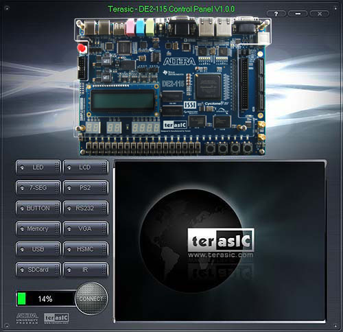 DE2-115 System BuilderDE2-115 System Builder – a powerful tool that comes with the DE2-115 board. This tool will allow users to create a Quartus II project file on their custom design for the DE2-115 board. The top-level design file, pin assignments, and I/O standard settings for the DE2-115 board will be generated automatically from this tool. In addition, through the GPIO and HSMC connectors you can select various daughter cards in conjunction with the DE2-115 using the DE2-115 System Builder. 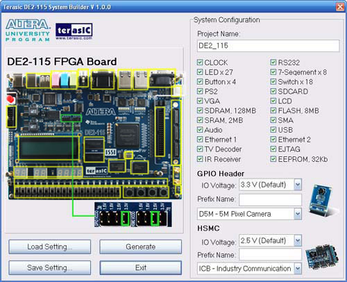 Related course resources:School: Universidad Pontificia BolivarianaInstructor:Prof. Holguer A. Becerra Course 1: - [Publication] Signal processing and waves graphing acceleration using FPGA School: University of Cambridge Professor: Simon Moore Course 1: -CHERI: a research platform deconflating hardware virtualization and protection Other course resources you might interested:School: Cornell UniversitySenior Lecturer: Bruce Land Course 1: - ECE5760 Advanced Microcontroller Design and system-on-chip [DE2] Course 2: - ECE 5760 Simplified Floating Point for DSP [DE2] Navigation MenuSearch code, repositories, users, issues, pull requests..., provide feedback. We read every piece of feedback, and take your input very seriously. Saved searchesUse saved searches to filter your results more quickly. To see all available qualifiers, see our documentation . - Notifications You must be signed in to change notification settings
A web application to easily lookup pin assignments of the Altera DE2 board. neelabhg/easy-de2-pin-assignmentsFolders and files. Repository files navigationEasy de2 pin assignments. A web application to easy search for pin assignments for Altera's DE2 board, and copy them into Altera's Quartus II.  Follow along with the video below to see how to install our site as a web app on your home screen. Note: This feature may not be available in some browsers. Welcome to EDAboard.comWelcome to our site edaboard.com is an international electronics discussion forum focused on eda software, circuits, schematics, books, theory, papers, asic, pld, 8051, dsp, network, rf, analog design, pcb, service manuals... and a whole lot more to participate you need to register. registration is free. click here to register now.. - Digital Design and Embedded Programming
- PLD, SPLD, GAL, CPLD, FPGA Design
Altera pin assignment- Thread starter shaiko
- Start date Jun 17, 2015
- Jun 17, 2015
Advanced Member level 5Hello, Altera's Quartus has 3 ways to assign pins to the FPGA device: 1. Assignment Editor. 2. Pin Planner. 3. Direct text input into *.QSF. My question: Are these tools synchronized with each other? For example: if I do initial assignments using the Pin Planner and then make changes in the *.QSF file - will the changes in the QSF propagate back to the Pin Planner settings?  Super ModeratorAs long as you save the changes to the QSF, I 'm pretty sure they get loaded for each tool (you may have to close and reopen the tool to get the latest changes), but I might be mis-remembering as it's been 5-6 years since I've used Quartus. TrickyDickyAdvanced member level 7. Any changes you make via assignment editor and pin planner are written to the QSF file (stands for quartus settings file I think). Quartus uses the QSF file to set up the assignment editor and pin planner (and all the other stuff in its gui). Ensure you havent got the project open when you hand edit the .qsf though You can also assign pins via attributes in the HDL. TrickyDicky said: Ensure you havent got the project open when you hand edit the .qsf though Click to expand... Similar threads- Started by hexaeder
- Mar 18, 2024
- Started by Oscar99haha
- Jul 31, 2022
- Started by latebird
- Feb 22, 2022
- Started by matrixofdynamism
- Dec 13, 2022
- Started by aminpix
- May 29, 2024
Part and Inventory SearchWelcome to edaboard.com. - This site uses cookies to help personalise content, tailor your experience and to keep you logged in if you register. By continuing to use this site, you are consenting to our use of cookies. Accept Learn more…
 | | | |


IMAGES
COMMENTS
DE2_Pin_Table.xls. Signal Name. FPGA Pin No. Description. SW[0] PIN_N25. Toggle Switch[0] SW[1] PIN_N26.
DE2-115 Board I/O Pin Assignments: Switches, LEDs, and 7-Segment Displays Table 1: Pin assignments for slide switches
Table 2: Pin assignments for slide switches DE2-115 Board I/O Pin Assignments: Switches, LEDs, and 7-Segment Displays
DE2-70 User Manual 1 Chapter 1 DE2-70 Package The DE2-70 package contains all components needed to use the DE2-70 board in conjunction with a computer that runs the Microsoft Windows software.
DE2 Board I/O Pin Assignments: Switches, LEDs, and 7-Segment Displays. Table 1: Pin assignments for toggle switches. Table 2: Pin assignments for pushbutton (debounced) switches. Table 3: Pin assignments for LEDs.
View and Download Altera DE2-115 user manual online. DE2-115 computer hardware pdf manual download.
Learn about the pinout, datasheet, and specifications of the Altera DE2-115 development board, which features the Cyclone IV E FPGA and various interfaces. See how to power up the board and access the control panel and demonstrations.
In addition, all these clock inputs are connected to the phase locked loops (PLL) clock input pins of the FPGA to allow users to use these clocks as a source clock for the PLL circuit. The clock distribution on the DE2-115 board is shown in Figure 4-11. The associated pin assignments for clock inputs to FPGA I/O pins are listed in Table 4-5.
The pin assignments between the Cyclone II FPGA and the VGA connector are listed in Table 4.8. An example of code that drives a VGA display is described in Sections 5.2 and 5.3.
Software Installation The Top-level Verilog Module and Pin Assignment 4-5 The complete top-level pin assignment is provided in C:\DE2\DE2_TOP project Please use the pin assignment in DE2_TOP project as golden pin assignment for all your projects.
View and Download Altera DE2 Board getting started manual online. Development and Education Board. DE2 Board motherboard pdf manual download.
Prelab Assignments Review the manual and tutorials for the Altera DE2 Board. Understand how to create and compile projects. Review how pin assignments are done. Review how to program the Altera DE2 Board. Lab Assignments Part 1 Create a new Quartus II project for your circuit.
Program the DE2 Board: Pin Assignments. We want to assign the two input pins to two of the switches on the DE2 board. If we look at the DE2 board schematic we have 18 switches to choose from and even more LEDS for output. For ease lets use switches 0 & 1 and led 0. These are located on the FPGA at pins N26, N25 & AE22 respectively.
View and Download Altera DE2-70 user manual online. Development and Education Board. DE2-70 computer hardware pdf manual download.
The DE2 board has a default set of pin assignments (and associated pin names) in DE2_pin_assignments.csv. Your life will be much easier if you import this file and use the variable names assigned by the developer.
4. Pin Assignment The DE2 board has hardwired connections between the FPGA pins and the other components on the board. We will use two toggle switches, labeled SW0, SW1and SW2, to provide the external inputs, a, b and cin, to our example circuit. These switches are connected to the FPGA pins N25, N26 and P25, respectively.
Terasic Inc. - Expertise in FPGA/ASIC Design
3. Pin Assignment The DE2 board has hardwired connections between the FPGA pins and the other components on the board. For this project, we need to access LED, LCD. 7-Segment LEDs and serial port. The wrapper file already mapped the input and output pins to their default names as used by alter pin assignment file.
However, the DE2 board has hardwired connections between the FPGA pins and the other components on the board. Pin assignments are made by using the Assignment Editor. Select Assignments >Pins to reach the window in Figure 16. Under Category select Pin to reach window in Figure 17.
A web application to easily lookup pin assignments of the Altera DE2 board. - neelabhg/easy-de2-pin-assignments
DE2-115 System Builder - a powerful tool that comes with the DE2-115 board. This tool will allow users to create a Quartus II project file on their custom design for the DE2-115 board. The top-level design file, pin assignments, and I/O standard settings for the DE2-115 board will be generated automatically from this tool.
Easy DE2 Pin Assignments A web application to easy search for pin assignments for Altera's DE2 board, and copy them into Altera's Quartus II.
Hello, Altera's Quartus has 3 ways to assign pins to the FPGA device: 1. Assignment Editor. 2. Pin Planner. 3. Direct text input into *.QSF. My question: Are these tools synchronized with each other? For example: if I do initial assignments using the Pin Planner and then make changes in...